Knowing how a bare board is made explains most of the design rules you are given. A minimum track width, a minimum hole size and a minimum ring of copper around a hole are not arbitrary: each comes from a step below. The order described is for a typical multilayer board with plated holes; processes differ in detail between factories.
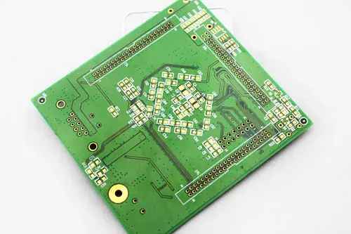
1. Engineering preparation
Before anything is cut, the factory's engineers read your files, check them against the process, and prepare production data. They fit your board onto a larger production panel, add test coupons and fiducials at the panel edge, and adjust features for the process: for example, they make copper slightly wider to compensate for what the etching removes. Questions you receive at this point are about the files.
What can go wrong: a missing layer, a wrong outline, or features the process cannot make. Mistakes caught here cost nothing.
2. Cutting the laminate
Copper-clad laminate comes in large sheets. It is cut into panels of the working size. For a multilayer board, the thin inner cores are cut too.
3. Inner layers: imaging and etching (multilayer only)
The copper on an inner core is covered with a light-sensitive film (photoresist). A pattern of your layer is exposed to light on the film, either through a film mask or by direct imaging with a laser. The unexposed or the exposed film (depending on the type of film) is washed away, leaving copper uncovered where it must be removed. The panel goes through an etching bath, which dissolves the exposed copper. The remaining film is stripped, and what is left is the copper pattern.
What can go wrong: etching sideways under the film makes tracks narrower than drawn (undercut), and very thin gaps may not clear. This is why the minimum track and gap exist.
4. Inner layer inspection
An automated optical inspection (AOI) compares each inner layer with your data. Shorts and opens found here are scrapped or repaired. After lamination they cannot be seen again.
5. Lamination
The cores are treated so that resin will stick to the copper, then stacked with sheets of prepreg (partly cured glass cloth) between them and copper foil on the outside. The stack goes into a heated press, which melts the resin and cures it under pressure into one solid panel.
What can go wrong: layers shifted against each other (registration error), voids in the resin, or bow and twist from an unbalanced stack. This is why a symmetric stack-up is good practice.
Steps 1 to 5, as small pictures.
- Step 1, engineering preparation: your board fitted on a production panel, with fiducials and a test coupon.
- Step 2, cutting: the laminate cut to the working size.
- Step 3, inner layers: light through the film hardens the resist; etching removes the copper that is not covered.
- Step 4, inner layer inspection: a camera compares each layer with your data.
- Step 5, lamination: cores and prepreg pressed into one panel.
6. Drilling
Holes are drilled through the panel with a spinning carbide bit, using a drill file. Very small holes are drilled with small bits, which break easily and are drilled one panel at a time or in thin stacks, so small holes cost more. Some very small holes are made by laser instead.
What can go wrong: drill wander, so holes are off-centre, and the ring of copper around a hole (the annular ring) gets too thin or breaks out at one side. A hole whose depth is many times its diameter (a high aspect ratio) is hard to plate in the next step.
7. Cleaning the holes and making them conductive
The drilled hole walls are smeared with resin and have no copper. A chemical step cleans out the smear. Then a thin layer of copper is deposited on the whole panel, including inside the holes, by a chemical process without current (electroless copper).
8. Plating copper
The panel is electroplated to build copper onto the thin chemical layer, so that the hole walls carry a robust copper barrel. This is the step that makes the plated hole a connection between layers, and it also thickens the surface copper.
What can go wrong: voids in the barrel, or thin plating in deep holes. These show up as intermittent connections after thermal cycling.
9. Outer layers: imaging and etching
The outer layers are imaged with photoresist as the inner layers were. The usual method is pattern plating: the resist leaves the tracks and pads open, those areas are plated with copper and then with a thin layer of tin, which acts as an etch resist. Then the resist is stripped and the copper that is not covered by tin is etched away, then the tin is removed. (Another method, tent and etch, protects the tracks with resist and etches the rest.)
10. Solder mask
The panel is coated with mask, which is exposed through your mask layer, developed, and cured. See Solder mask, silkscreen and via treatments.
What can go wrong: mask on pads from misregistration, bridges between fine pads lost, ink in holes that should stay open.
Steps 6 to 10.
- Step 6, drilling: a bit drills through the panel.
- Step 7, cleaning and a thin copper layer over the whole panel, hole walls included.
- Step 8, plating: copper is built up into a robust barrel and onto the surface.
- Step 9, outer layers: the tracks are tinned as an etch resist, and the other copper is etched away.
- Step 10, solder mask: over the tracks, open at the pads.
11. Surface finish
The exposed copper receives its finish: hot air solder leveling, immersion gold over nickel, an organic film, and so on. See Surface finishes compared.
12. Silkscreen
The legend is printed over the mask and cured. Ink on pads is a defect.
13. Profiling: routing and scoring
The panel is cut into boards. A router follows your outline, and leaves small tabs if the boards stay in a panel. Alternatively a V-shaped groove is cut halfway through from both sides (V-scoring) so that boards can be snapped apart. Slots, cut-outs and edge plating happen here too. See Panelisation and small boards.
What can go wrong: routing too close to copper, exposing it at the edge.
14. Electrical test
Every board is tested for continuity and isolation against the netlist built from your files. Two methods are used: a flying probe tester, with moving probes, which needs no fixture and suits prototypes and small runs; and a fixture with many fixed pins (a bed of nails), which is faster for larger runs and costs more to set up. The test finds opens and shorts. It does not find a design error: it tests that the board matches your files, not that your files match your circuit.
15. Final inspection and packing
Boards are inspected visually, measured for thickness and size, and checked against the order. Some factories cut microsections from test coupons, to check the plating and the layers. The boards are baked if required, vacuum packed with desiccant, and packed.
Steps 11 to 15.
- Step 11, surface finish on the exposed copper.
- Step 12, legend printed over the mask.
- Step 13, profiling: the router follows the outline and leaves tabs, or a groove is cut between boards.
- Step 14, electrical test: probes touch pads and check for opens and shorts.
- Step 15, final inspection and packing.
What you can take from this
- Fine features reduce yield at imaging and etching, so they cost more.
- Small holes, deep holes and thin rings are risks at drilling and plating.
- Layers must be balanced and registered, or the board warps.
- A board that passes electrical test is built as drawn. Whether the drawing is right is yours to review.
How this shows up when you order here
The 25 checks at upload look at the same things the production engineer looks at in step 1: missing layers, an open outline, holes that miss their pads, features below what the process makes, and the match between the files and what you ordered. The limits are on the capabilities page. An engineer confirms every order before production starts. To follow what happens to the finished bare board, read How boards are assembled.